< img height="1" width="1" style="display:none" src="https://www.facebook.com/tr?id=26825290190466607&ev=PageView&noscript=1" />

Nullam dignissim, ante scelerisque the is euismod fermentum odio sem semper the is erat, a feugiat leo urna eget eros. Duis Aenean a imperdiet risus.

Dental-burs-1
Dental-burs-3
Dental-burs-2
Dental-burs-1
Dental-burs-3
Dental-burs-2

CVD Diamond Dental burs

Micron-level precision cutting, balancing ultimate wear resistance with a gentle clinical experience,This series of dental burs features a high-purity integrated stainless steel/carbide substrate, coated with advanced CVD nano-diamond (or high-density natural diamond grit electroplating). Engineered for high-intensity clinical procedures such as tooth preparation, cavity access, decay removal, cosmetic restoration (veneer prep), and crown/bridge cutting. The ultra-hard, uniformly distributed diamond coating delivers aggressive cutting efficiency while minimizing frictional heat to protect the dental pulp, making it the premium choice for modern digital dentistry.
  • Ultra-hard and wear-resistant for extended service life
  • Sharp cutting performance for high efficiency and reduced operator fatigue
  • Precise shaping for fine dental procedures
  • Heat-resistant and non-burning
  • Biocompatible and clinically safe
  • Broad compatibility and versatile application

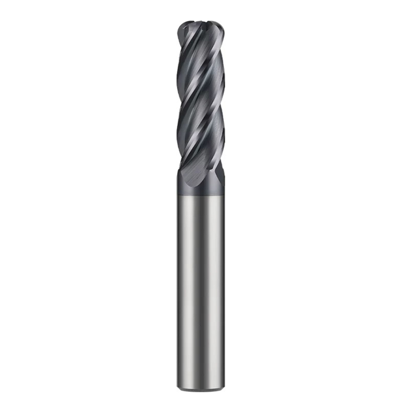
The Secret to Long-Life Zirconia Milling: Why TSHZ Diamond Burs are the Premium Choice for Dental Labs

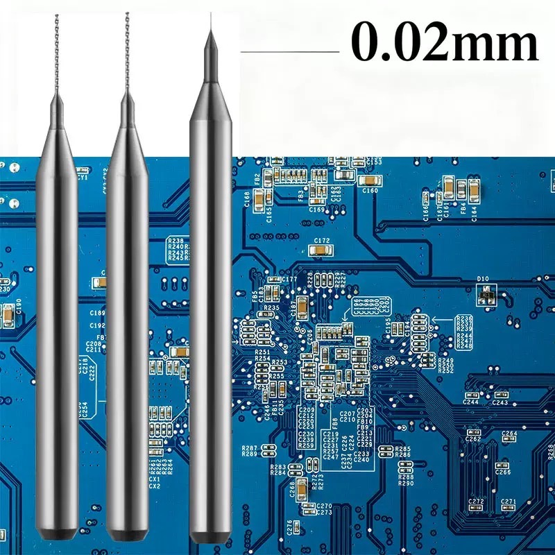
In digital dentistry, the precision of CAD/CAM milling is the bridge between a digital scan and a perfect clinical fit. However, Zirconia—even in its pre-sintered state—is highly abrasive. Standard tungsten carbide burs dull rapidly, leading to micro-chipping at the critical margin areas (the thin edges of crowns and veneers).

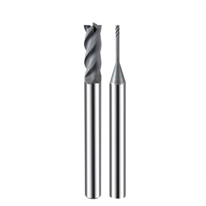
Tiansheng Hengzuan (TSHZ) has engineered a specialized line of CVD Diamond Coated Dental Burs. By applying a pure crystalline diamond layer, we solve the two most expensive problems in dental labs: premature tool failure and edge integrity loss.

1. Solving the Pain Points of Dental Milling

1、Marginal Chipping: As a bur wears down, cutting forces increase, causing “shattering” at the thin cervical margins. This leads to poor fitment and increased manual rework.

2、Color Contamination: Low-quality coatings can flake off during high-speed milling. These metallic residues can compromise the translucency and shade accuracy of the zirconia during sintering.

3、Low Throughput: Frequent tool changes disrupt unattended milling cycles, reducing the total units produced per shift.

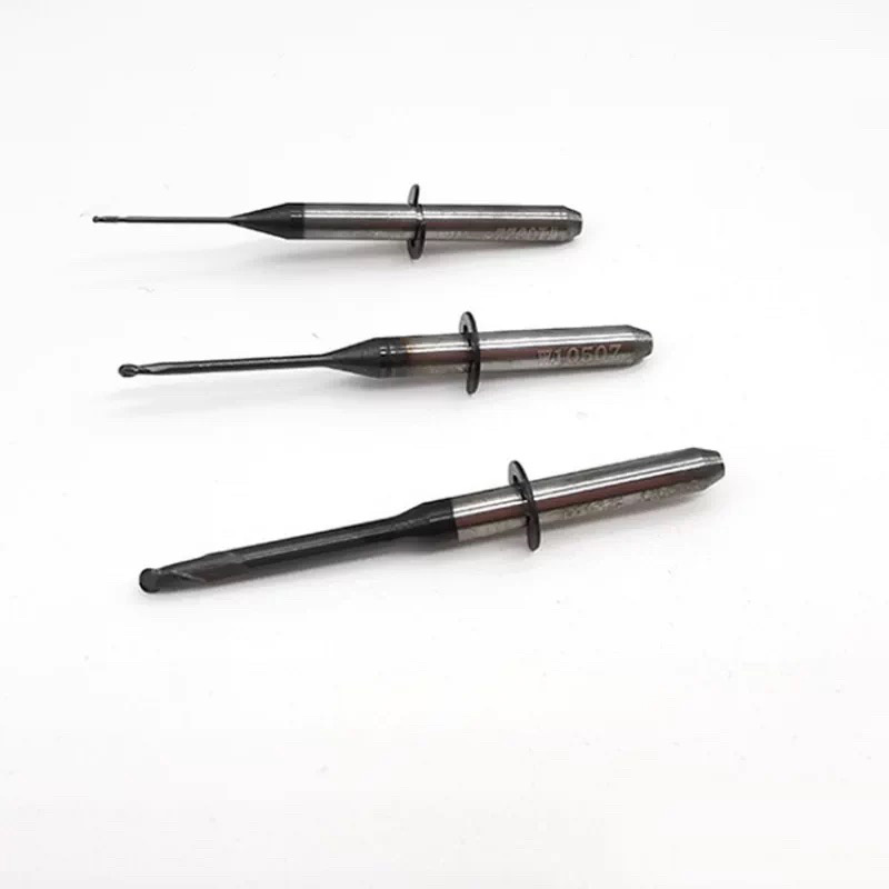
2. Technical Specializations of TSHZ Dental Burs

A. 10,000 HV Hardness: 500+ Units Per Bur

Using Chemical Vapor Deposition (CVD), we grow a high-purity polycrystalline diamond film directly onto the carbide shank.

Performance: Wear resistance is 8-10 times higher than standard coatings.

The ROI: Depending on the material hardness, a single TSHZ bur can stably process over 500 units, drastically lowering the tool cost per crown.

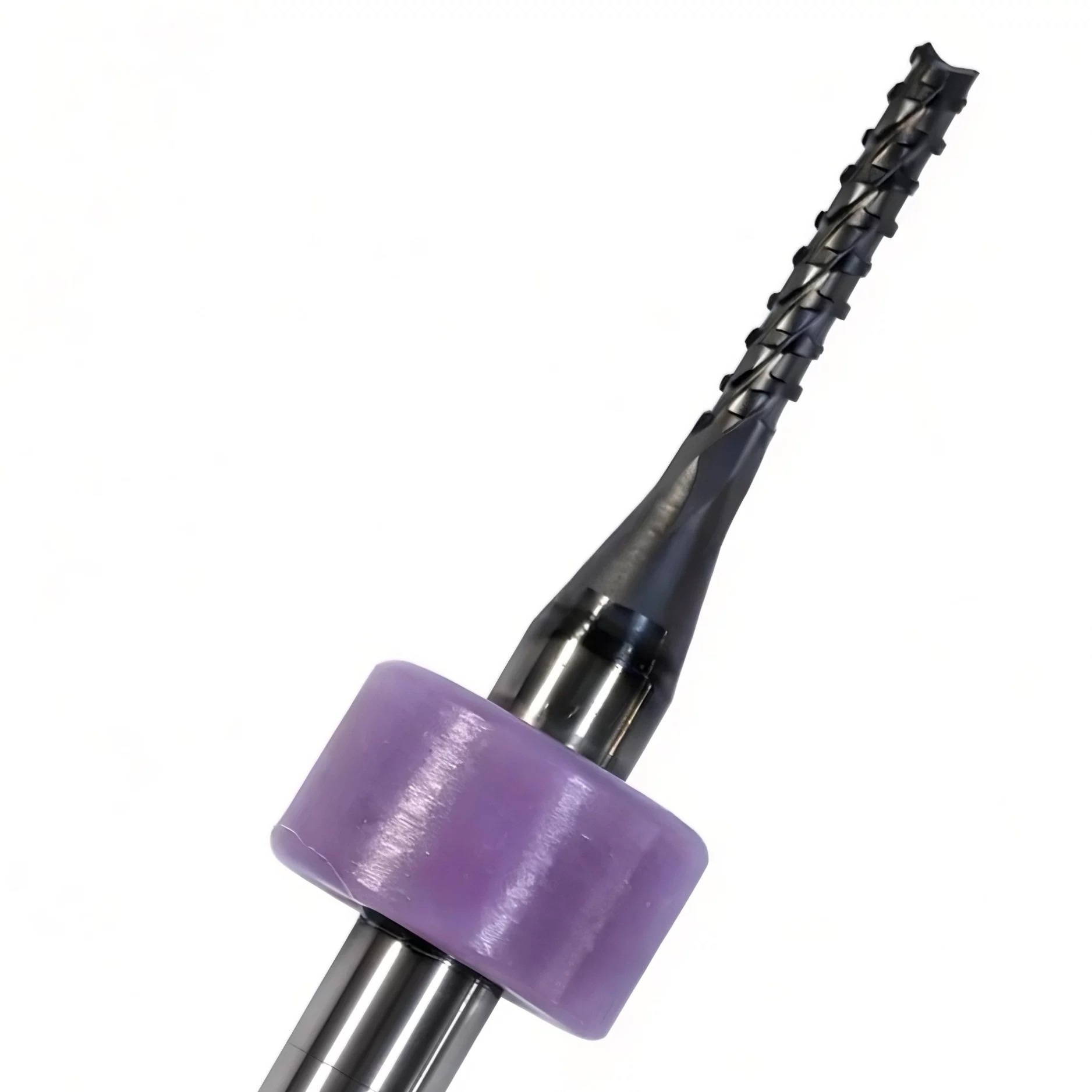
B. Mirror Finish & Low Friction (< 0.1)

Milling zirconia creates a massive amount of fine dust that can stick to the cutting edge, leading to heat buildup.

Seamless Evacuation: Our diamond coating features an ultra-low friction coefficient (< 0.1). Combined with our optimized flute design, zirconia powder is evacuated like a fluid, preventing Built-Up Edge (BUE).

Aesthetic Superiority: The smooth cutting action ensures the milled surface is fine and uniform, reducing the time required for post-milling polishing.

C. 10-15μm Uniform Coating for Precision Margins

For 0.6mm or 0.3mm burs used in fissure and margin detailing, coating uniformity is everything.

Precision Control: TSHZ uses a proprietary thickness compensation technique to ensure a uniform 10-15μm layer across the entire ball-end geometry.

The Result: Perfect reproduction of delicate veneer margins without chipping, ensuring a seamless fit for the patient.

D. Zero Heavy Metal Contamination

Our CVD process is strictly controlled to ensure a pure carbon diamond layer, free from impurities.

Bio-Safety: There is zero metal migration during the milling process, preserving the natural translucency and shade of the zirconia after sintering, meeting all medical-grade requirements.

3. Recommended Milling Parameters (Zirconia Optimized)

To maximize the life of your diamond burs, we recommend the following parameters for standard CAD/CAM systems:

Bur Diameter (mm) Recommended RPM Feed Rate (mm/min) Primary Function
φ2.0 / φ2.5 18,000 – 25,000 1,200 – 2,000 Roughing (Opening)
φ1.0 25,000 – 35,000 800 – 1,200 Semi-Finishing
φ0.6 / φ0.3 35,000 – 45,000 400 – 600 Margin & Fissure Detailing

4. Conclusion: Efficiency is Your Best Strategy

In the competitive dental lab industry, throughput and quality are the only metrics that matter. Tiansheng Hengzuan (TSHZ) Diamond Burs are more than just tools—they are an insurance policy for your finished crowns.

Don’t let a dull bur ruin a perfect design. Choose TSHZ for surgical precision and unmatched longevity.

PRODUCTS

PRODUCTS

View More
PCB-diamond-drill-bit

PCB diamond drill bit

PCB drill bits with excellent chip removal and hole roughness capabilities, long service life, suitable for drilling general multilayer and HDI boards, FR-4, CEM-1 boards, and eco-friendly boards. Diameter range: 0.1–3.175 mm,For the latest PCB boards, diamond-coated drills achieve over 3,000 holes per bit.
Learn More
PCB-Diamond-Coated-Milling-Cutters-1

PCB Diamond-Coated Milling Cutters

PCB diamond-coated milling cutters, also known as PCB routing cutters, printed circuit board milling cutters, or engraving cutters, are primarily used for contour cutting, slotting, depth-controlled milling, V-grooving, half-hole machining, and gold finger chamfering of PCBs; they are the most commonly used carbide tools in post-PCB manufacturing processes.
Learn More
Flat-bottom-cylindrical-end-mill-1

Diamond coating Flat-bottom cylindrical end mill

Standard 2-flute/4-flute design with sharp cutting edges and large chip clearance space, suitable for efficient roughing and semi-finishing of graphite electrodes.
Learn More
Round-Nose-End-Mill

Diamond coating Round Nose End Mill

Balances the corner-clearing capability of flat-end mills with the chipping resistance of ball-end mills, extending tool tip life and enabling rapid roughing of cavities.
Learn More
Our Blog

Blog

View More

12/ May

What is the biggest bottleneck for global AI computing power? It is a drill bit with a diameter of less than 0.2 millimeters.

Everyone is obsessing over Nvidia’s GPUs and HBM memory. But here is the cold truth about 2026: The biggest threat to global AI server delivery isn’t a chip shortage or a lack of light modules. It is a needle—a micro-drill bit less than 0.2mm in diameter. Think about it. We are building “Cathedrals of Computation” that cost billions, yet their survival depends on whether we can drill 100,000 perfect holes in a high-density backplane without snapping a single needle. In the world of AI, 0.01mm of deviation isn’t an error; it’s a total system collapse. Why is this happening now? Because Nvidia’s new architectures (Rubin/Rubin Ultra) have pushed PCB materials to the physical limit. We’ve moved from standard FR-4 to M9 high-frequency materials filled with 99.99% silica—essentially drilling through quartz. The tool life has plummeted from 2,000 holes to barely 200. This is no longer “manufacturing”; it is atomic-scale carving. If your tool provider doesn’t understand the micro-physics of CVD coatings, your production line is a ticking time bomb.     To secure your position in the AI supply chain, stop looking at “Price per Tool” and start looking at these three technical moats: 1.Aspect Ratio Mastery (50:1): For 8mm thick boards, you need a 50x aspect ratio. Only a handful of companies globally can maintain verticality at this scale. Ensure your supplier uses Gradient CVD Diamond Coatings to manage the thermal shock that exceeds 800℃ at the tip. 2.Equipment Autonomy: The global lead time for Swiss-made high-precision grinders is now 18 months. If your supplier doesn’t manufacture their own CNC grinding equipment, they cannot scale with your demand. Vertical integration is the only hedge against supply chain paralysis. 3.Substrate Decobaltization Depth: Check the chemical treatment of the tungsten steel substrate. For AI-grade M9 materials, you need a precise decobaltization depth to ensure the diamond coating doesn’t peel under high-frequency friction. The AI revolution is loud, but the real winners are those mastering the silence of the laboratory. But the reality is extremely cruel and absurd: in 2026, the fate of global AI computing power will be determined by a “toothpick” with a diameter of less than 0.2 millimeters, thinner than a human hair. This is an extremely pathological phenomenon. We can design a GPU capable of trillions of operations per second, yet often a $5 diamond drill bit deviating by just 0.01 millimeters during drilling can cause an entire AI server backplane, worth a fortune, to be scrapped. This is not precision manufacturing; it’s like defusing a bomb in the microscopic world. In 2026, the biggest failure for a PCB Procurement Director isn’t paying too much—it’s buying “garbage” that kills the factory’s yield. Most people don’t realize that the AI server boards for NVIDIA aren’t just “thicker”; they are physically “hostile” to traditional tools. When you use a standard tungsten needle on M9 high-frequency material, you aren’t manufacturing; you are committing “industrial suicide.” A deviation of 0.01mm—the width of a ghost—and a 50,000 backplane becomes scrap metal. In this era, “cheap” is the most expensive mistake you can make.     As a Procurement Director, you must enforce these three “Hard-Core” technical filters to protect your margins: Demand the “SP3 Bond Density” Certificate: Don’t settle for “Diamond-like” claims. Real CVD Diamond coatings must have an SP3 content that hits a hardness of 80-100 GPa. Insist on a Raman Spectroscopy report. Only a high SP3 peak ensures the drill won’t soften under extreme friction, allowing you to hit 2,000 holes instead of 200. Verify “Nano-scale Decobaltization” Depth: Diamond and Tungsten are naturally incompatible. Premium tools require a chemical decobaltization process at a specific nano-depth. If the substrate isn’t treated perfectly, the coating will peel off like “dead skin” under stress. Ask for the “Gradient Interface” specs; this is the difference between a tool that lasts a shift and one that snaps in seconds. Audit the “Honing Radius” Precision: Thicker coating is a trap. If it’s too thick, the cutting edge becomes rounded, skyrocketing the cutting force and shattering the board. The gold standard is a post-coating edge radius (Honing) strictly under 2 μm If the Ra (Roughness) of the hole wall doesn’t hit nano-levels during testing, reject the batch immediately. 4.In the age of AI, the Procurement Director is the factory’s “Technical Firewall.” The battle for AGI isn’t just about silicon; it’s about that unbreakable, 0.2mm needle forged in a vacuum.      At TSHZ (Tiansheng Hengzhuan), we don’t sell consumables; we sell the “Skeletal Support” for the world’s most powerful servers. If you’re tired of explaining scrap rates to your boss, let’s talk. Real solutions aren’t found in the “lowest price” column—they are grown in the lab, atom by atom.
Learn More
PCB drilling

26/ April

Stop the $5 Price War: Join the CVD Diamond Revolution and Capture the 2026 Blue Ocean.

Headline: Dominate the High-End Market: TSHZ Global Recruitment for CVD Diamond Tool Distributors The Context: Manufacturing in Vietnam, Thailand, and Malaysia is shifting from “low-cost assembly” to “high-precision engineering.” While your competitors are fighting a price war over $5 carbide mills, are you ready to offer the “1 = 20” Diamond Solution that ends the competition? Why TSHZ is the Ultimate Tool for SEA Distributors: The “Japan/Germany” Alternative: Our performance rivals top-tier global brands, but our pricing structure allows you to capture the market aggressively. Give your clients premium quality without the premium price tag. The AI Server Boom: As PCB manufacturing for AI servers migrates to Southeast Asia, the demand for high-layer count drilling is exploding. TSHZ Diamond Drills are the only solution for “Zero Smear” and “Zero Breakage” in 32-layer boards. Full-Scale Empowerment: We provide more than just tools. You get our full library of viral marketing videos (FB/TikTok), technical white papers, and 24/7 engineering support from our Shenzhen HQ. The Market is Blue. The Opportunity is Now. Most distributors are still sleeping on CVD technology. Be the first in your region to bring the “Industrial Tooth” of 2026 to your clients. [CTA]: DM for the “SouthEast Asia Partner Growth Kit” and request your trial samples today.
Learn More
bannner-3

25/ April

Beyond Silicon: Why a Few Grams of Lab-Grown Crystals in Jiangxi Will Redefine High-End Manufacturing

1. The “Cold War” in the Lab: Why Diamonds are the Ultimate Frontier While the world fixates on the scarcity of “luxury diamonds,” a more strategic battle is unfolding in the laboratories of Shenzhen Tiansheng Hengzhuan Technology. For their engineers, diamonds are not jewelry—they are the “Ultimate Semiconductor.” As silicon-based chips approach their physical limits (Moore’s Law), and Gallium Nitride (GaN) reaches its thermal ceiling, the industry is pivoting toward a “Heat-Sink Savior.” The upcoming National Key Laboratory for Diamond Materials in Jiujiang, Jiangxi, is not just a research center; it is a declaration of war against the “Thermal Barrier” in high-power electronics. 2. A Strategic Convergence: Shenzhen’s “Brain” Meets Jiujiang’s “Hand” Why would a high-tech powerhouse from Shenzhen’s tech hub relocate its crown jewel—a National Key Lab—to Jiujiang, Jiangxi? This is a calculated Supply Chain Symbiosis. Tiansheng’s “Cognitive Edge”: With dozens of patents in CVD (Chemical Vapor Deposition) growth and precision doping, Tiansheng understands that the next bottleneck for 5G base stations, deep-sea probes, and military radar is not logic, but Heat Dissipation. Jiujiang’s “Industrial Depth”: Jiangxi’s strategic layout in advanced materials provides more than just policy incentives. It offers a stable energy grid and a manufacturing ecosystem capable of scaling lab breakthroughs into industrial reality. 3. Inside the Lab: Cracking the “Anti-Human” Challenges of Physics This lab isn’t chasing headlines; it’s chasing the limits of atomic physics. Here are the three technical pillars Tiansheng is fortifying: I. The Thermal Conductivity Gamble Diamonds possess the highest natural thermal conductivity (over $2000 W/m·K$), five times that of copper. Tiansheng’s mission is to achieve large-area, high-purity diamond wafer fabrication. This requires simulating “Subterranean Extremes” in a vacuum, forcing carbon atoms to align with sub-nanometer precision. II. The “Forbidden Zone” of N-type Doping Diamonds are natural insulators. Turning them into semiconductors requires “Doping”—a process akin to modern alchemy. Tiansheng’s lab is tackling the stability of N-type phosphorus doping, a hurdle that has stumped global researchers for decades. Success here means processors that can operate at $500^{\circ}C$ without melting. III. The Cost Revolution via Laser Peeling A lab is only as good as its commercial viability. The Jiujiang facility is refining proprietary Laser Lift-Off (LLO) and non-destructive grinding techniques. By slashing the cost of diamond substrates, Tiansheng aims to transition this “Black Tech” from orbital satellites to everyday smart EVs. 4. The Stakes: What Happens If We Fail? In the race for hypersonic flight, quantum computing, and long-range radar, the winner won’t be the one with the best software, but the one with the best Material Science. By planting this flag in Jiujiang, Tiansheng Hengzhuan is executing a “Dimensional Strike” on traditional semiconductor paths. While others patch up silicon-based systems, Tiansheng is digging trenches in the “No-Man’s Land” of diamond electronics. 5. Elevating Value: The Era of “Deep Tech” Patience This news isn’t just about corporate expansion; it’s about a shift in the industrial zeitgeist. In an era of “Quick Capital,” Tiansheng has chosen the arduous path of fundamental science. These few grams of lab-grown crystals will eventually serve as the “Skeletal System” for the next generation of global high-end equipment.
Learn More
Factory-Display3

1/ April

Sustainable Manufacturing Trend: Diamond Coating Listed as a Key Technology for “Green Machining”

Global manufacturing’s environmental requirements will reach a new high in 2026. Due to their exceptionally long service life, CVD diamond tools significantly reduce the carbon footprint associated with discarded tools and enable higher-efficiency dry machining (reducing cutting fluid pollution), leading multiple governments to include them on their recommended lists for sustainable manufacturing.
Learn More
Industry-News-5
Get Standed
Is your tooling keeping up with the "Difficult-to-Machine" era?

Leave A Message

Graphite, Ceramics, and Carbon Fiber are the future, but they are “tool killers.” If you’re still using traditional coating, you’re fighting a losing battle.
Our CVD (Chemical Vapor Deposition) Diamond Coating creates a real crystalline diamond layer on the carbide substrate. This isn’t just a “finish”—it’s a shield.

Why top distributors choose our CVD series:
1.Ultra-Low Friction: Prevents chip welding and heat buildup.
2.Extreme Abrasion Resistance: Maintains sharp cutting edges $20 \times$ longer.
3.Surface Finish: Mirror-like results on the workpiece, zero secondary polishing needed.

    Your Name*

    Email

    Tel

    WhatsApp*

    Message

    Products
    Contacts
    WhatsApp
    Email