25 , April
1. The “Cold War” in the Lab: Why Diamonds are the Ultimate Frontier
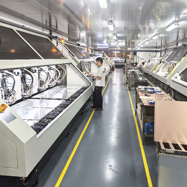
While the world fixates on the scarcity of “luxury diamonds,” a more strategic battle is unfolding in the laboratories of Shenzhen Tiansheng Hengzhuan Technology. For their engineers, diamonds are not jewelry—they are the “Ultimate Semiconductor.” As silicon-based chips approach their physical limits (Moore’s Law), and Gallium Nitride (GaN) reaches its thermal ceiling, the industry is pivoting toward a “Heat-Sink Savior.” The upcoming National Key Laboratory for Diamond Materials in Jiujiang, Jiangxi, is not just a research center; it is a declaration of war against the “Thermal Barrier” in high-power electronics.
2. A Strategic Convergence: Shenzhen’s “Brain” Meets Jiujiang’s “Hand”
Why would a high-tech powerhouse from Shenzhen’s tech hub relocate its crown jewel—a National Key Lab—to Jiujiang, Jiangxi? This is a calculated Supply Chain Symbiosis.
Tiansheng’s “Cognitive Edge”: With dozens of patents in CVD (Chemical Vapor Deposition) growth and precision doping, Tiansheng understands that the next bottleneck for 5G base stations, deep-sea probes, and military radar is not logic, but Heat Dissipation.
Jiujiang’s “Industrial Depth”: Jiangxi’s strategic layout in advanced materials provides more than just policy incentives. It offers a stable energy grid and a manufacturing ecosystem capable of scaling lab breakthroughs into industrial reality.
3. Inside the Lab: Cracking the “Anti-Human” Challenges of Physics
This lab isn’t chasing headlines; it’s chasing the limits of atomic physics. Here are the three technical pillars Tiansheng is fortifying:
I. The Thermal Conductivity Gamble
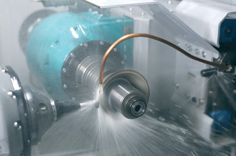
Diamonds possess the highest natural thermal conductivity (over $2000 W/m·K$), five times that of copper. Tiansheng’s mission is to achieve large-area, high-purity diamond wafer fabrication. This requires simulating “Subterranean Extremes” in a vacuum, forcing carbon atoms to align with sub-nanometer precision.
II. The “Forbidden Zone” of N-type Doping
Diamonds are natural insulators. Turning them into semiconductors requires “Doping”—a process akin to modern alchemy. Tiansheng’s lab is tackling the stability of N-type phosphorus doping, a hurdle that has stumped global researchers for decades. Success here means processors that can operate at $500^{\circ}C$ without melting.
III. The Cost Revolution via Laser Peeling
A lab is only as good as its commercial viability. The Jiujiang facility is refining proprietary Laser Lift-Off (LLO) and non-destructive grinding techniques. By slashing the cost of diamond substrates, Tiansheng aims to transition this “Black Tech” from orbital satellites to everyday smart EVs.
4. The Stakes: What Happens If We Fail?
In the race for hypersonic flight, quantum computing, and long-range radar, the winner won’t be the one with the best software, but the one with the best Material Science.
By planting this flag in Jiujiang, Tiansheng Hengzhuan is executing a “Dimensional Strike” on traditional semiconductor paths. While others patch up silicon-based systems, Tiansheng is digging trenches in the “No-Man’s Land” of diamond electronics.
5. Elevating Value: The Era of “Deep Tech” Patience
This news isn’t just about corporate expansion; it’s about a shift in the industrial zeitgeist. In an era of “Quick Capital,” Tiansheng has chosen the arduous path of fundamental science. These few grams of lab-grown crystals will eventually serve as the “Skeletal System” for the next generation of global high-end equipment.