Nullam dignissim, ante scelerisque the is euismod fermentum odio sem semper the is erat, a feugiat leo urna eget eros. Duis Aenean a imperdiet risus.
Nullam dignissim, ante scelerisque the is euismod fermentum odio sem semper the is erat, a feugiat leo urna eget eros. Duis Aenean a imperdiet risus.
 author
While the world fixates on the scarcity of “luxury diamonds,” a more strategic battle is unfolding in the laboratories of Shenzhen Tiansheng Hengzhuan Technology. For their engineers, diamonds are not jewelry—they are the “Ultimate Semiconductor.” As silicon-based chips approach their physical limits (Moore’s Law), and Gallium Nitride (GaN) reaches its thermal ceiling, the industry is pivoting toward a “Heat-Sink Savior.” The upcoming National Key Laboratory for Diamond Materials in Jiujiang, Jiangxi, is not just a research center; it is a declaration of war against the “Thermal Barrier” in high-power electronics.
Why would a high-tech powerhouse from Shenzhen’s tech hub relocate its crown jewel—a National Key Lab—to Jiujiang, Jiangxi? This is a calculated Supply Chain Symbiosis.
Tiansheng’s “Cognitive Edge”: With dozens of patents in CVD (Chemical Vapor Deposition) growth and precision doping, Tiansheng understands that the next bottleneck for 5G base stations, deep-sea probes, and military radar is not logic, but Heat Dissipation.
Jiujiang’s “Industrial Depth”: Jiangxi’s strategic layout in advanced materials provides more than just policy incentives. It offers a stable energy grid and a manufacturing ecosystem capable of scaling lab breakthroughs into industrial reality.
This lab isn’t chasing headlines; it’s chasing the limits of atomic physics. Here are the three technical pillars Tiansheng is fortifying:
Diamonds possess the highest natural thermal conductivity (over $2000 W/m·K$), five times that of copper. Tiansheng’s mission is to achieve large-area, high-purity diamond wafer fabrication. This requires simulating “Subterranean Extremes” in a vacuum, forcing carbon atoms to align with sub-nanometer precision.
Diamonds are natural insulators. Turning them into semiconductors requires “Doping”—a process akin to modern alchemy. Tiansheng’s lab is tackling the stability of N-type phosphorus doping, a hurdle that has stumped global researchers for decades. Success here means processors that can operate at $500^{\circ}C$ without melting.
A lab is only as good as its commercial viability. The Jiujiang facility is refining proprietary Laser Lift-Off (LLO) and non-destructive grinding techniques. By slashing the cost of diamond substrates, Tiansheng aims to transition this “Black Tech” from orbital satellites to everyday smart EVs.
In the race for hypersonic flight, quantum computing, and long-range radar, the winner won’t be the one with the best software, but the one with the best Material Science.
By planting this flag in Jiujiang, Tiansheng Hengzhuan is executing a “Dimensional Strike” on traditional semiconductor paths. While others patch up silicon-based systems, Tiansheng is digging trenches in the “No-Man’s Land” of diamond electronics.
This news isn’t just about corporate expansion; it’s about a shift in the industrial zeitgeist. In an era of “Quick Capital,” Tiansheng has chosen the arduous path of fundamental science. These few grams of lab-grown crystals will eventually serve as the “Skeletal System” for the next generation of global high-end equipment.
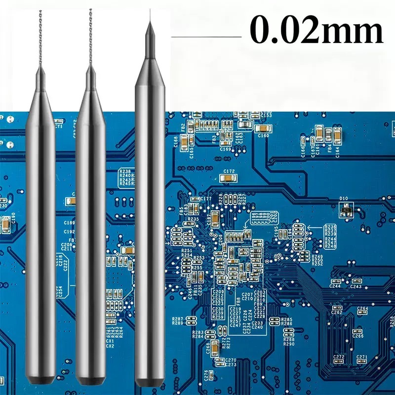
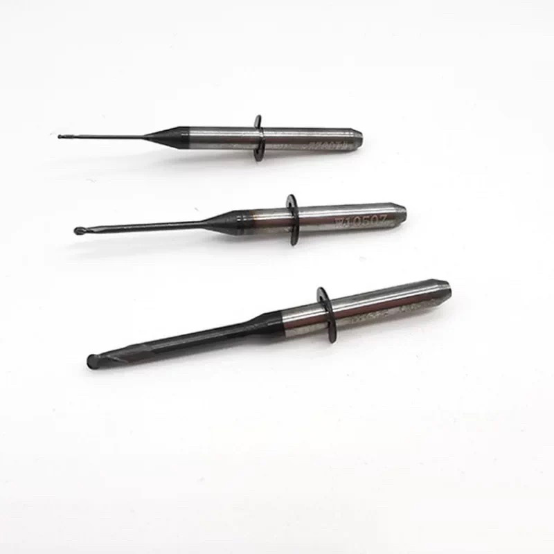
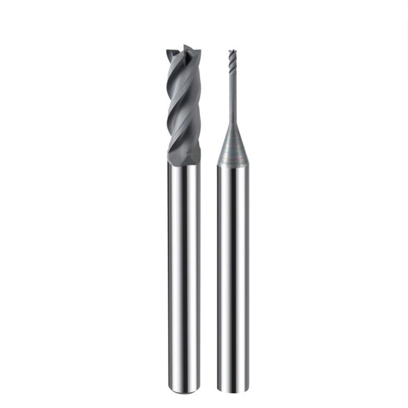
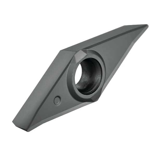
Graphite, Ceramics, and Carbon Fiber are the future, but they are “tool killers.” If you’re still using traditional coating, you’re fighting a losing battle.
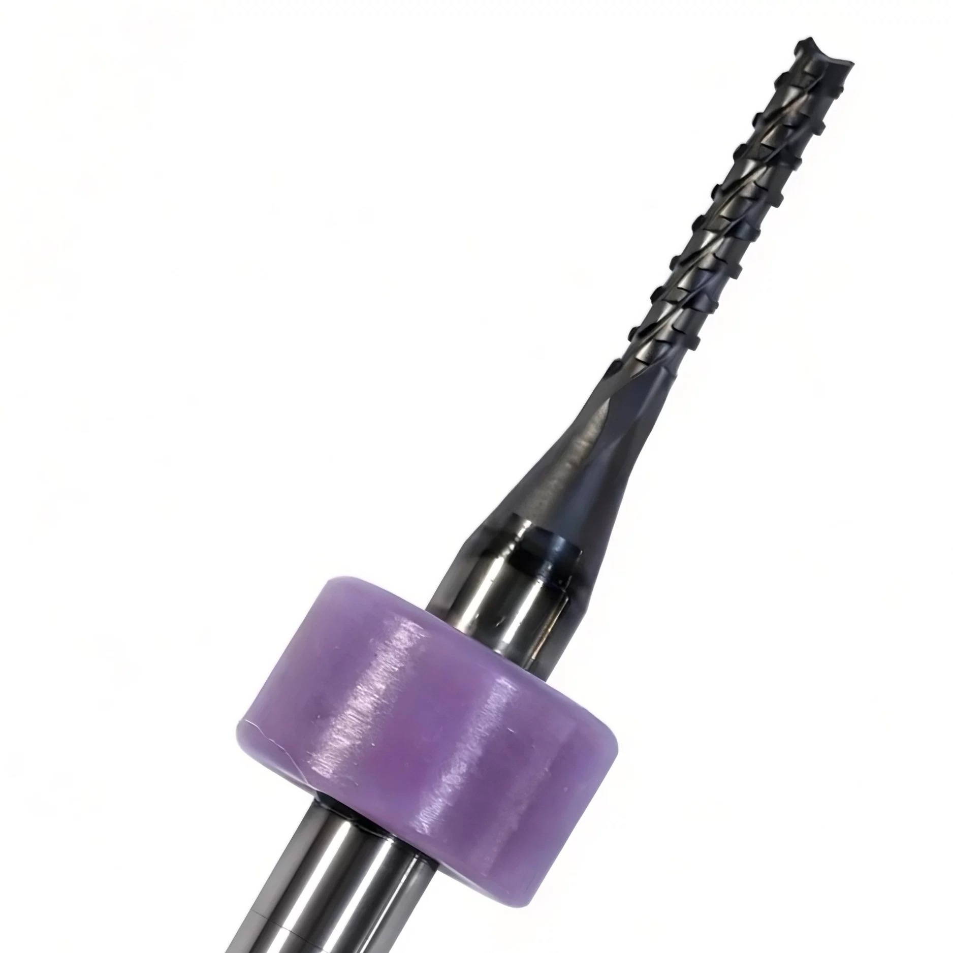
Our CVD (Chemical Vapor Deposition) Diamond Coating creates a real crystalline diamond layer on the carbide substrate. This isn’t just a “finish”—it’s a shield.
Why top distributors choose our CVD series:
1.Ultra-Low Friction: Prevents chip welding and heat buildup.
2.Extreme Abrasion Resistance: Maintains sharp cutting edges $20 \times$ longer.
3.Surface Finish: Mirror-like results on the workpiece, zero secondary polishing needed.


