
Complete Guide: CVD Diamond Coated Micro Drills & End Mills for PCB Manufacturing
1. Critical Machining Defects of PCB Substrates
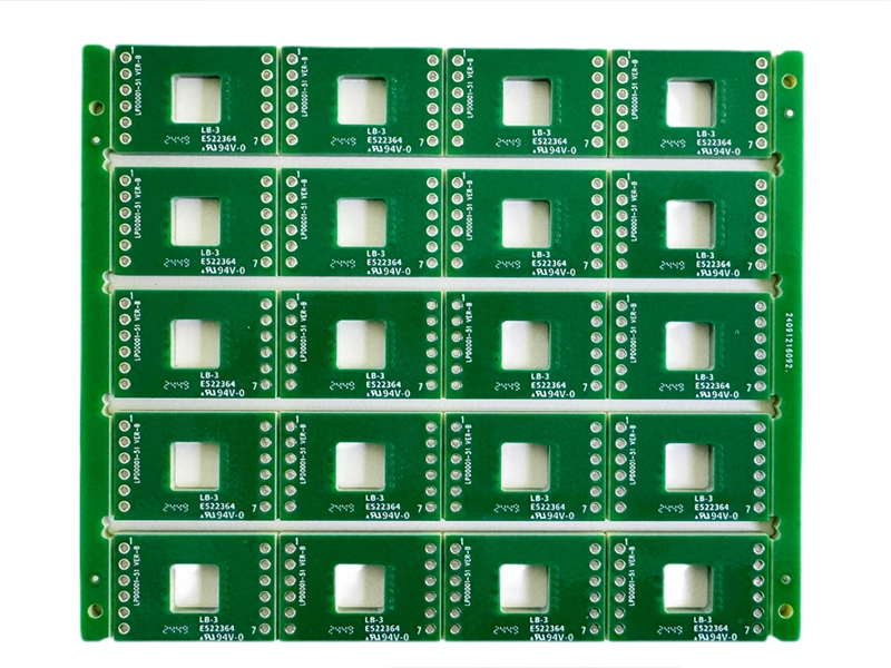
The mainstream PCB substrate is glass fiber reinforced epoxy FR-4, together with high-frequency ceramic-filled PTFE laminates, M7/M8/M9 high-speed boards, IC packaging substrates, HDI high-density interconnect boards, aluminum substrates and flexible FPC materials. These composite materials are filled with abrasive quartz fiber & ceramic particles, bringing severe limitations to uncoated carbide tools:
- Extremely short tool service lifeStandard carbide micro drills only process hundreds of holes on regular FR-4 before edge rounding. For M9 high-frequency boards with hard ceramic fillers, carbide drills fail after merely 100–200 holes. Frequent tool changes reduce drilling machine utilization and raise overall consumable costs sharply.
- Severe delamination, fiber burrs & copper foil liftingSharp glass fibers are pulled rather than cut by dull carbide edges, resulting in entry spalling, exit delamination and massive hole wall burrs. Inner copper foils of multi-layer boards tear easily, causing electroplating voids and short circuits, which heavily lower yield of AI server PCBs.
- Resin carbonization & rough hole walls caused by accumulated heatTungsten carbide features poor thermal conductivity. Heat concentrates at tiny drill tips during microvia drilling, melting and blackening epoxy resin. Rough hole walls increase signal loss, failing the electrical standards of 5G and computing motherboards.
- High breakage rate of micro drills & unstable dimensional tolerance0.05–0.3mm ultra-small drills have weak rigidity. Tool wear creates unbalanced cutting force, leading to hole diameter deviation and position drift. Thin substrates are scrapped due to drill breakage in mass production.
- Heavy deburring workload after routing & profilingCarbide routing cutters leave frayed edges and ply separation on PCB outlines. Manual deburring is mandatory for every panel, raising labor cost and blocking fully automatic production lines.
2. Unique Advantages of CVD Diamond Coated Tools for PCB
- Extreme abrasion resistance multiplies tool lifespanDiamond hardness reaches 9000–10000 HV, far exceeding tungsten carbide, resisting persistent abrasion from glass fiber and ceramic fillers. Tool life extends 5–10 times on FR-4, 10–20 times on ceramic-filled M9 high-frequency boards. Each diamond drill stably processes over ten thousand microvias, cutting tool change downtime and lowering cost per hole by over 30%.
- Superior thermal conductivity eliminates resin burningDiamond thermal conductivity is dozens of times higher than carbide, rapidly evacuating heat at drill tips to prevent epoxy carbonization. Smooth hole walls minimize signal attenuation, fully meeting strict electrical requirements of high-frequency PCBs and IC substrates.
- Long-lasting sharp edges eliminate delamination & burrsDense smooth diamond coating retains sharp cutting edges throughout the tool lifetime, cutting glass fibers cleanly instead of pulling them. Micro-level burr control avoids hole edge damage and drastically improves finished PCB yield, removing manual deburring steps.
- Uniform coating on ultra-small & high length-diameter ratio toolsCVD deposition evenly coats micro drills starting from 0.05mm diameter, extended blind hole drills, profiling cutters and step drills. It solves the limitation of brazed PCD tools which cannot be manufactured into miniature geometries, covering blind vias, microvias, slotting and full panel routing processes.
- Low-friction smooth flutes for stable chip evacuation & less breakageSmooth diamond surface repels glass dust and resin debris to prevent flute clogging. Cutting resistance is reduced significantly, lowering micro drill breakage rate and ensuring consistent hole dimension accuracy in mass batches.
3. Custom Tool Selection by PCB Material
- Standard FR-4 double & multi-layer PCBNano-crystal CVD diamond micro drills & 2-flute profiling end mills, balanced wear resistance and cost for consumer electronics & power board mass production.
- HDI high-density interconnect boards & blind buried viasThin-edge nano diamond step micro drills with low cutting pressure to suppress thin panel delamination, ideal for 0.1–0.3mm micro through holes.
- M7/M8/M9 high-speed boards & ceramic-filled PTFE (5G & AI server motherboards)Thick microcrystalline diamond coated drills with enhanced anti-abrasion performance against hard ceramic fillers, maintaining ultra-smooth hole walls for high-frequency signal transmission.
- IC packaging substrates & ABF carriersUltra-fine grain diamond ultra-small drills with razor-sharp edges, delivering micron-level precision for advanced packaging micro hole machining.
- PCB aluminum substrate slotting & contour routingAnti-adhesion diamond coated routing cutters to stop aluminum & copper foil built-up edge, avoiding circuit scratches from metallic chips.
4. Recommended Machining Parameters for PCB Production
Microvia Drilling
Spindle speed: 30,000–120,000 RPMFeed per tooth fz: 0.01–0.06 mm/zOperation: Dry cutting or minimal mist lubrication with synchronous high-power vacuum dust extraction
PCB Routing & Slot Milling
Cutting speed Vc: 200–500 m/minFeed per tooth fz: 0.04–0.15 mm/zMilling type: Climb milling, full vacuum panel clamping to eliminate vibration-induced delamination
5. Main Application Industries
AI computing server PCB, 5G communication high-frequency circuit boards, new energy vehicle automotive PCBs, consumer electronics laptop & mobile motherboards, HDI phone substrates, semiconductor IC packaging carriers, industrial control circuit boards, wind power inverter boards.
6. Operation Notes & Restrictions
- Glass fiber dust irritates skin and respiratory tracts; high-power vacuum dust extraction system is required on all PCB production lines.
- Never machine ferrous metal, cast iron or titanium alloy with diamond coated tools. Ferrous elements chemically erode diamond film under high cutting temperature and cause coating peeling.
- Only applicable to glass fiber composite laminates and ceramic-filled non-metallic substrates; thick pure copper panels are not recommended for diamond cutting tools.
- Ultra-small micro drills must be matched with high-rigidity high-precision drilling machines to reduce machining vibration and extend coating service life.
- Clean spindle and worktable dust regularly to avoid hard glass particles scratching diamond coating surfaces.