
Nullam dignissim, ante scelerisque the is euismod fermentum odio sem semper the is erat, a feugiat leo urna eget eros. Duis Aenean a imperdiet risus.
Nullam dignissim, ante scelerisque the is euismod fermentum odio sem semper the is erat, a feugiat leo urna eget eros. Duis Aenean a imperdiet risus.
 author
“Burrs on edge” is too vague for the next operator: an FR-4 profile may show curled copper, exposed glass fibres or chipped laminate. Record each defect separately and photograph the edge before trimming it or changing the router.
At a glance: Name the defect, mark its position on the board drawing and photograph both faces and the cut wall before cleanup. Check router condition, holder seating, support and extraction. Then change one approved variable at a time and inspect the same locations against the same acceptance rule.
This procedure concerns external profile routing; drilling and microvias require different tool and quality checks. Keep the board drawing, router specification and machine instructions available at the workstation.
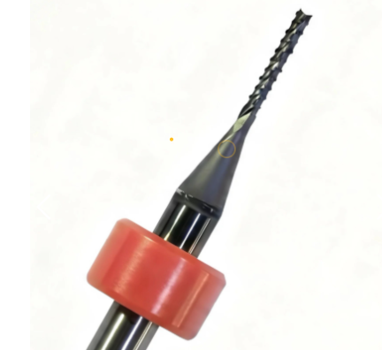
A PCB routing burr is excess material or a raised edge left after a circuit-board profile is cut. On FR-4, distinguish a copper lip from exposed glass fibres, resin cracking or a local chip. Record its location, inspect the tool and support, then compare a repeat sample before changing a cutting parameter.
| Edge observation | Record before cleanup | First useful comparison |
| Copper curled over one face | Face, entry or exit side, and affected length | Same profile location on a repeat board |
| Glass fibres sticking out of the wall | Direction, location and inspection view | Matching wall section under the same light |
| Resin crack or laminate chip | Position near entry, corner, tab or support change | Same point on a retained sample |
| Defect varies across a stack | Board order and support condition | Same layer position and restraint |
Issuing a board that violates its drawing or shop acceptance requirement while identifying the cause; conclusive actions are not required for release decisions. Keep a board that violates its drawing or shop acceptance rule as you chase the cause; you do not have to find root-cause before making your release decision.
Prior to the deburring process take photographs of: The top face, underside and cut wall with each defect marked out on a drawing. Separated out findings such as record curled copper at entry or exit, projecting fibres with cracked/missing resin. Examine the same sites in uniform illumination on both samples so that a difference of vision cannot be mistaken for actual process improvement.

A top-view photograph can conceal cut-wall damage, while a generic “rough edge” label groups unlike defects and leaves the next operator without a clear investigation target.
Since FR-4 consists of glass fibres, resin and copper foil, one profile can have different types of defects. On the review setup, isolate face to record copper and exposed-fibre section; or a cracked/missing laminate. Document the copper-face, open-fibre and broken or absent laminate in isolation prior to evaluating the configuration.
Glass-fibre direction and heat influence machining damage in composites. In a controlled GFRP study, trochoidal milling cut cycle time by up to 23% in the tested setup (GFRP milling study). Conventional milling produced better dimensional control and a finer finish in certain fibre-sensitive regions. FR-4 is a different beast; these results call for further investigation of exposed fibres, not follow-on recommendation on PCB feed.
Inspect the same marked location on the next board under consistent lighting and magnification, noting whether the defect appears only on the underside. A general “poor edge quality” judgment can hide that diagnostic pattern.
Mark the start and end of each damaged section on the drawing, including its relationship to entries, exits, corners, tabs and support changes. Repeated damage beside a tab suggests a different investigation from a defect extending along the full profile.
| What you see | What to record next |
| Copper curled over one face | Which face, where, and on how many boards |
| Fibres exposed along the wall | Direction, length of edge and inspection view |
| Resin cracks or a local chip | Position relative to entry, exit, corner or tab |
| Different results across a stack | Board order and support at the inspected location |
If the edge misses the drawing, hold the board under the shop’s quality procedure while the root-cause investigation proceeds.
Save Off the arrangement that made suspect edge: router id, holder and support and permitted machine settings before changing feed. If both cutter and fixture have changed, Clean Edge cannot tell which correction counted. Retain sufficient level of detail to allow repeatable run. Keep sufficient baseline detail so that you can repeat the run.
Runout is the change in radial distance you see when rotating a mounted tool. This will be dictated by the procedure and limits set forth by the machine maker — document which tool/tooling is to used with this reading, along with how it was setup. The same reference-condition perspective is invoked when a measurement method changes; the NIST measurement-process guide explains how reference conditions and variability affect comparisons.
Remove the router under the machine’s maintenance procedure and inspect the cutting edge. Check seating and runout by the maker’s method and limits. A tolerance from another machine may not apply to this spindle.
A dull edge can contribute to resin micro-cracks, exposed fibres or chipped laminate. Check it, but do not treat the edge alone as proof of cause. Also check board construction, backing, toolpath and setup. If the router’s service history is missing, mark it unknown and choose a traceable fresh tool for the baseline comparison.
Routine regrinding is not recommended for a diamond-coated router. It can damage the coating and expose the lower-hardness carbide beneath. Ask the supplier whether an approved refurbishment path exists before sending a coated tool for sharpening. Keep the answer beside the tool record.
Photograph backing, restraint and extraction before unclamping, when those conditions are still visible. For a stack, identify each layer and its position before separation so the inspection record remains tied to the correct board.
A controlled routing trial compares samples while holding the inspection method and other relevant conditions steady. Settle the acceptance rule before cutting a trial board. The drawing and shop inspection procedure should say what passes. Mark spots another operator can find, then keep the light, magnification and handling the same for both samples. Inspect both sides the same way for a useful comparison.
The NIST guide to experimental design describes a simple discipline: decide what you will change and measure the result. Apply it to a routing trial, while recognizing that it will not explain every interaction:
Keep each marked spot’s result beside its photo. For example, a cleaner entry edge does not clear an exit that still misses the drawing. Repeat the comparison under the shop’s quality procedure before changing the production standard. The trial narrows the investigation; it cannot model every interaction in routing.
For profile work, cutting length may be more useful than board count when recorded alongside board type, stack details and inspection results. Length alone cannot explain an edge change without those operating conditions.
For external profiles, specify the operation first, then match the router geometry, diameter, working length and coating to the board and machine. Similar diameter does not make a drill interchangeable.
There is a difference between diamond-cut geometry and a diamond coating. Ask what geometry is proposed for the external profile, then ask about the coating separately. The word “diamond” on its own leaves both questions open.
TSHZ supplies CVD diamond coated PCB router bits. Across its milling-cutter range, listed operations include contour cutting, slotting, controlled-depth milling, V-shaped cutting, half-hole processing and gold-finger beveling. Those are range capabilities; check the individual model before matching it to a job.
For profile work, the diamond coated PCB router bits page is the natural starting point. Keep drilling and routing specifications apart, even where the diameters look alike.
For general background on cutter form and coating, see TSHZ’s tool geometry and coating explanation. Confirm a specific router against its model drawing.
The PCB milling-cutter range lists these diameter and length pairs. A router working length is the usable cutter length for the operation. Check the model drawing because catalogue symbols can differ:
| Diameter D (mm) | Catalogue length L (mm) |
| 0.8 | 6.0 |
| 1.0 | 7.0 |
| 2.0 | 10.0 |
| 3.175 | 15.0 |
Check the drawing for what “L” means on the exact model before ordering; do not assume it is overall length. The listed pairs belong to specific models and should not be mixed into new combinations.
Put board or stack thickness, reach and holder constraints on the drawing or inquiry. TSHZ offers standard-size tools and non-standard customization, but a custom tool still has to suit the job in front of it. Settle geometry and dimensions first, then run the edge comparison.
Send the supplier a marked drawing, photos of both faces and the cut wall, and the machine, holder and router identities. Include support and permitted settings, plus the usage record and any baseline sample. Label each sample with its setup; an isolated burr photograph cannot identify a suitable router.
Ask the supplier to tie the proposed model and trial plan to the acceptance requirement. When a sample passes, keep that result next to the tool revision and purchase record. The next shift can then repeat a known setup instead of trusting “the new bit looked better.”
When the drawing and trial notes are ready, request a model review through the TSHZ contact page. For company background, visit about us.
Coating alone does not guarantee an edge result on every board. Check the proposed router on the actual profile against the same acceptance rule, and bring holder and support checks into the trial when wear is a possible cause.
A matching diameter does not make a drill and a router interchangeable, so request a tool specified for lateral profile cutting and confirm the entry operation against the machine and tool instructions.
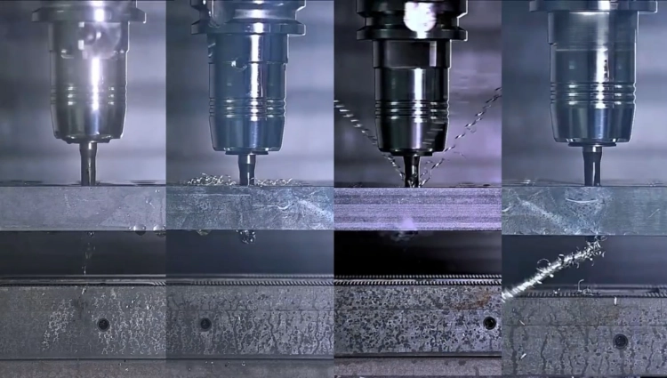
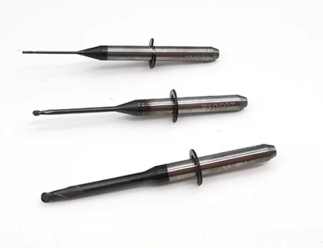
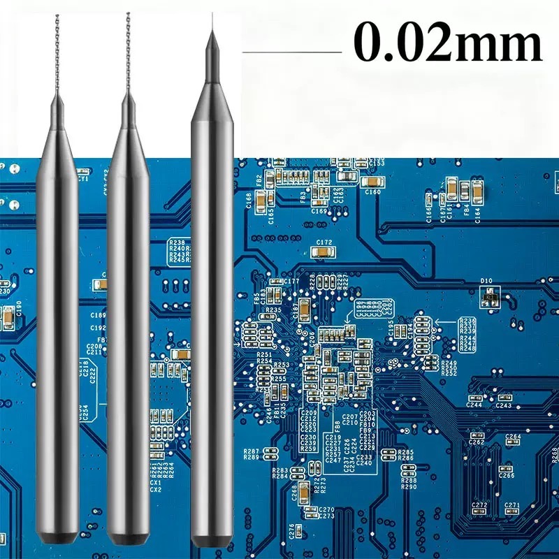
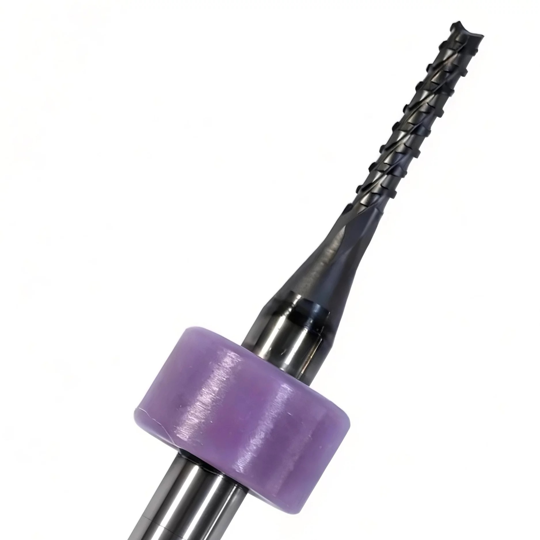
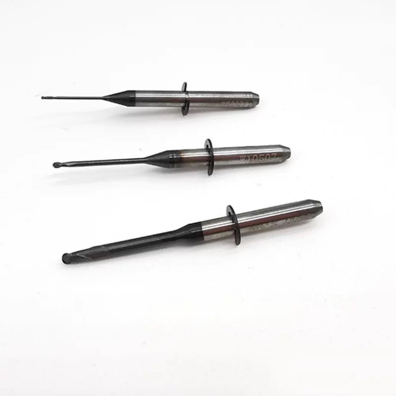
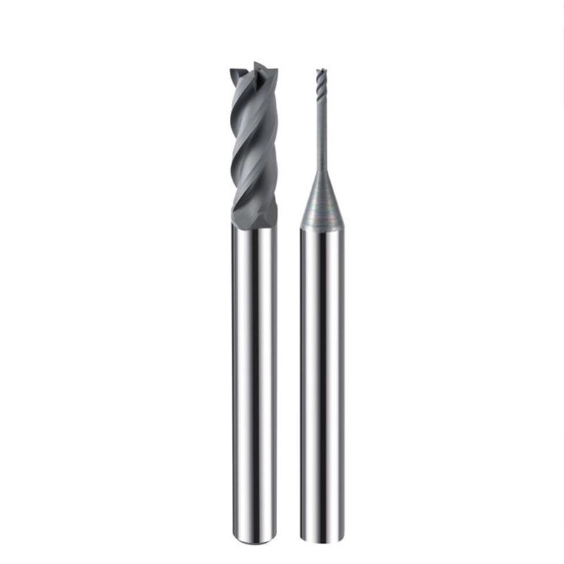
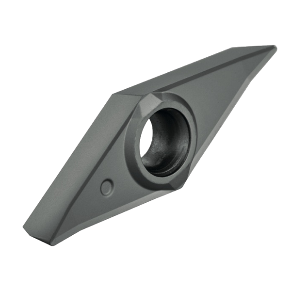
Graphite, Ceramics, and Carbon Fiber are the future, but they are “tool killers.” If you’re still using traditional coating, you’re fighting a losing battle.
Our CVD (Chemical Vapor Deposition) Diamond Coating creates a real crystalline diamond layer on the carbide substrate. This isn’t just a “finish”—it’s a shield.
Why top distributors choose our CVD series:
1.Ultra-Low Friction: Prevents chip welding and heat buildup.
2.Extreme Abrasion Resistance: Maintains sharp cutting edges $20 \times$ longer.
3.Surface Finish: Mirror-like results on the workpiece, zero secondary polishing needed.