
尊厳なんてない、セリリスクの前にはeuismod fermentumの憎しみがある sem semper はerat、feugeat leo urna eget erosです。デュイス・アネアン 笑いのためのヘアカット。
尊厳なんてない、セリリスクの前にはeuismod fermentumの憎しみがある sem semper はerat、feugeat leo urna eget erosです。デュイス・アネアン 笑いのためのヘアカット。
 著者
The first clue may be a rejected cross-section, not a rough-looking hole. Copper at an inner layer has bent or spread, although the board surface looks ordinary. In HDI and multilayer production, that is a different investigation from chasing a visible burr. Keep the suspect panel, record its place in the drill stack, and examine a section before changing the setup. Otherwise an apparent improvement after a tool change may simply reflect a different panel or a different point in the drill’s life.
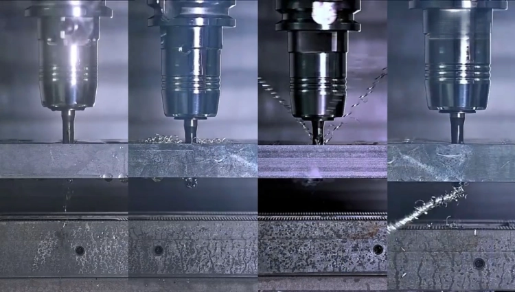
In FR-4, the edge passes through glass fiber, resin, and copper. Glass is abrasive, resin retains heat, and copper can deform rather than break cleanly. TSHZ identifies worn edges and copper pulled during drill withdrawal as nail-head mechanisms in PCB work. A worn drill may also leave rough walls or drift from its intended hole position. The inspection sheet should have separate entries for those faults. “Bad holes” gives the next shift almost nothing to work with.
Nail heading is deformation of copper at the inner-layer interface visible in a prepared hole cross-section. Save an image of the whole hole as well as a close view of the affected layer. Label the layer, panel, and drilling sequence on the image. A nearby acceptable hole from the same setup is a useful reference. Without it, “rough” or “pulled” can mean different things to the drilling and quality teams.
A number written into a supplier FAQ is not the acceptance limit for every PCB. Use the drawing and the plant’s inspection method. If the copper shape is borderline, identify the measurement points and retain the prepared section. Preparation damage can confuse the reading; section another hole if necessary. Changing feed before the feature is agreed upon wastes a trial.
An entry or exit burr sits at the board surface. Nail heading sits at buried copper. Resin smear is different again: softened resin can coat the wall and interfere with exposed copper. The University of Maryland CALCE explanation of resin smear helps identify that wall condition. Several faults may be present on one panel. Give each one its own photograph and description.
Write a separate note for the surface burr and the buried copper. Add wall condition and hole position. Which panel was cut? A technician repeating the inspection tomorrow should be able to find the same feature without guessing. If a trial makes the entrance clean but leaves the inner layer distorted, the work is not finished.
“Sample from the stack” is a poor label. Number the panels from top to bottom and put that number on each cross-section. An upper-panel failure that appears immediately may call for a fresh-tool or entry check; gradual deterioration down the stack points elsewhere. TSHZ’s PCB guidance warns that adding layers to a stack increases drill deflection risk and can reduce positional accuracy, especially with small diameters. A short drill is stiffer and less prone to wandering than an unnecessarily long one. Check both dimensions against the actual setup before deciding that nail heading is caused by wear alone.
The drilling traveler should identify entry and backing materials and how the panels were held. Measure actual drilling depth. Is the flute long enough to clear the full stack? Is the exposed drill longer than necessary? If coordinate data exist, compare hole position on upper and lower panels. A trend down the stack merits a setup check, even when edge wear is also visible.
Pick holes from the start and late part of the same drill run. Section them in the same way. A late sample with worse copper deformation is useful only if its laminate, hole size, and stack are known. Ask whether the wall has also become rougher or the hole position has moved. TSHZ recommends looking at hole-wall quality and visible edge wear when deciding when to replace a PCB micro drill. Keep the used edge with its sample record, rather than a tray of unlabelled drills.
The first holes are defective. That points to the setup before a wear-life discussion: was the specified drill fitted, did it seat correctly, what was the runout, and which entry and backing materials were used? Record feed, speed, and stack height. A defect that appears only much later has a different timeline; pull that drill and inspect its edge and flutes. Treating the two timelines as one problem makes both harder to solve.
Glass fiber in FR-4 abrades the edge; copper can be drawn into a deformed shape as the edge loses cutting ability or during withdrawal. In HDI drilling, carbide drill wear can coincide with nail heading, rough hole walls, and positional drift. That combination is a reason to examine the point and cutting edges, then match the edge photograph to the holes drilled with that tool. It is not a guarantee that another factory will see the symptoms in the same order.
Keep the first acceptable section and the last one before the defect limit is crossed. Put the corresponding edge images beside them. This gives purchasing and production a replacement point tied to their board, rather than a hole-count figure borrowed from another laminate. TSHZ also advises against routine regrinding of a diamond-coated micro drill because grinding can remove the coating and alter the edge geometry. If regrinding is attempted, its output belongs in a separate trial record.
The hole contains a difficult mix: abrasive glass fiber, insulating resin, and ductile copper. Resin’s poor heat conduction can leave local heat around a drill, while packed chips change contact at the edge. Pull the suspect drill and inspect the flutes for loading. Section a nearby hole to check for smear. Heat and chip removal may matter even if nail heading is the rejected feature. The Arlon drilling-defects technical note gives a useful reference for reading drill wear alongside cutting conditions.
There is a temptation to change everything when scrap is rising. Resist it for the short diagnostic run. Change feed, or stack, or tool type, then compare the same panel position. Four simultaneous changes may produce a good section without showing which one helped. The withdrawal setting belongs on the sheet as well; the copper can be pulled on the way out.
Measure runout at the fitted tool, not merely at an empty spindle. Check seating, spindle condition, and whether the stack lies flat. A short total length improves rigidity for PCB drilling; too many stacked panels increase deflection risk for small drills. That is a direction for testing, not a universal stack count. If one machine produces the damage and another does not, investigate the machine before assuming that the drill design is wrong.
On lower panels, look at the backing and the withdrawal move. On one suspect spindle, check the spindle. It sounds basic, yet a tool trial often arrives with no record of which copper layer was rejected. Attach two labelled sections to each change request: one before and one after. They will settle more than a note saying “new drill helped.”
TSHZ offers a PCB用ダイヤモンドドリルビット range for general multilayer and HDI boards. Its TS-A01UC micro drill is specified for HDI and multilayer work; the UC flute is intended to improve chip evacuation in dense small-hole drilling. It is worth trialling when worn edges or chip-packed flutes are part of the defect record. A fresh coated drill cannot compensate for a loose stack or a spindle running out.
Specify diameter and effective length against the finished-hole requirement, plating allowance, and actual stack. TSHZ also offers TS-A02 ST for standard FR-4/CEM work and TS-A03 for larger-diameter or thicker-board drilling. When comparing series, record the geometry and length as well as the coating; more than one property may have changed. The separate HDI and multilayer drill comparison covers that selection decision in more detail.

Run the candidate against the same laminate, stack, diameter, machine, and sectioning method as the current drill. Sample near the beginning and end of each tool run. Record the buried copper, surface burr, wall, hole position, and edge. An improved entrance with unchanged inner-layer distortion is an entrance improvement, not a nail-head solution. Extend the comparison far enough into the run to see whether the result holds.
An inquiry is easier to answer when it includes the laminate and board build, copper-layer arrangement, finished-hole target, current drill diameter and length, total stack, machine, and spindle. Attach edge and cross-section images labelled with panel position and hole count. Include feed, speed, withdrawal settings, and the board’s own acceptance requirement. TSHZ’s PCBアプリケーションページ covers the board-material context. The labelled samples show the precise failure under discussion.
No. Surface burrs appear at entry or exit. Nail heading is evaluated at an inner copper layer in a prepared hole cross-section. Report both if both are present.
No. The drill edge, flute, length, stack support, runout, and withdrawal condition all affect the result. A coated tool trial is most informative after the defect pattern has been documented.
A change in hole-wall quality, nail-heading trend, roughness, positional accuracy, or visible cutting-edge wear is a reason to review the replacement interval. Use the plant’s own inspection requirement and board construction rather than a copied universal hole count.
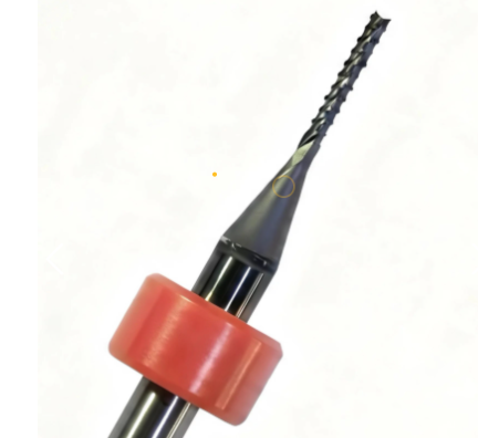
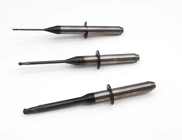

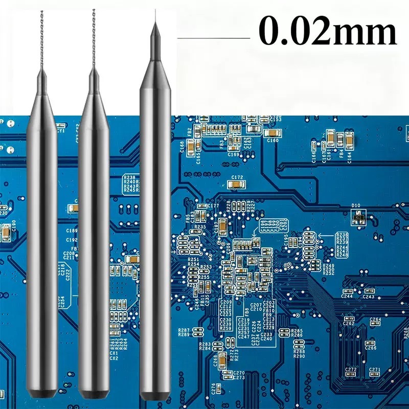
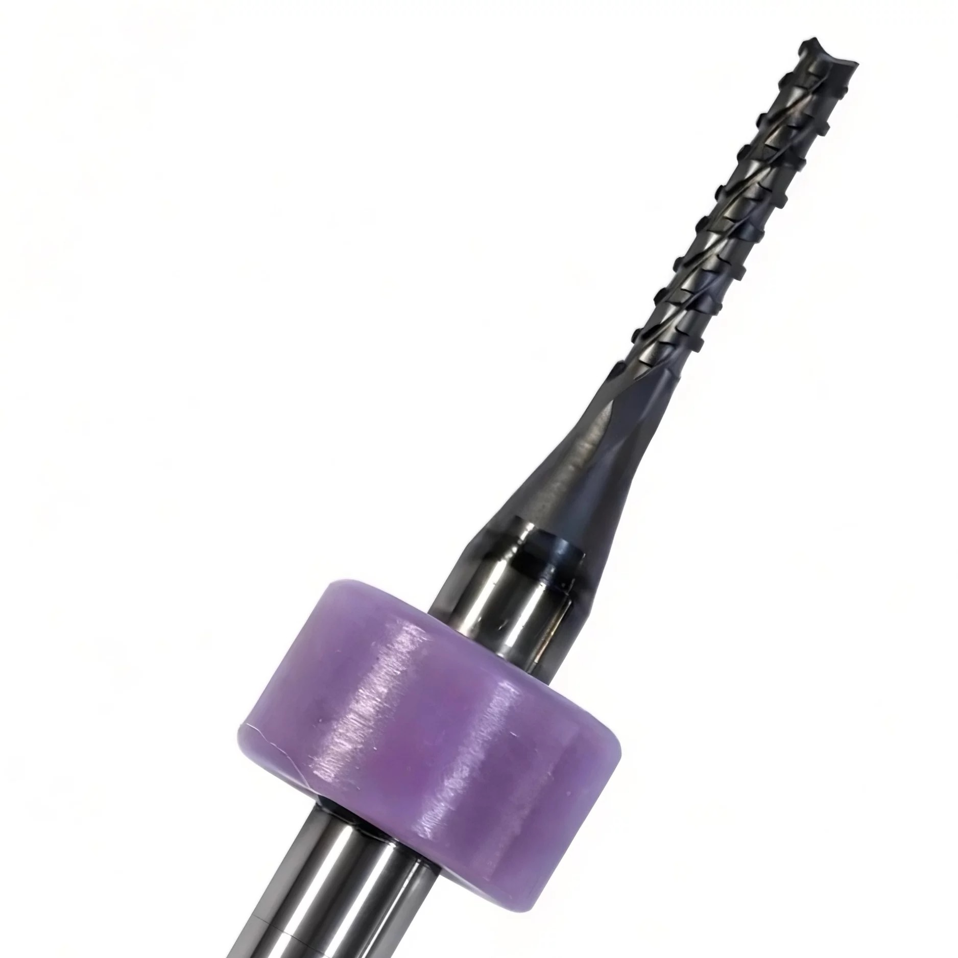
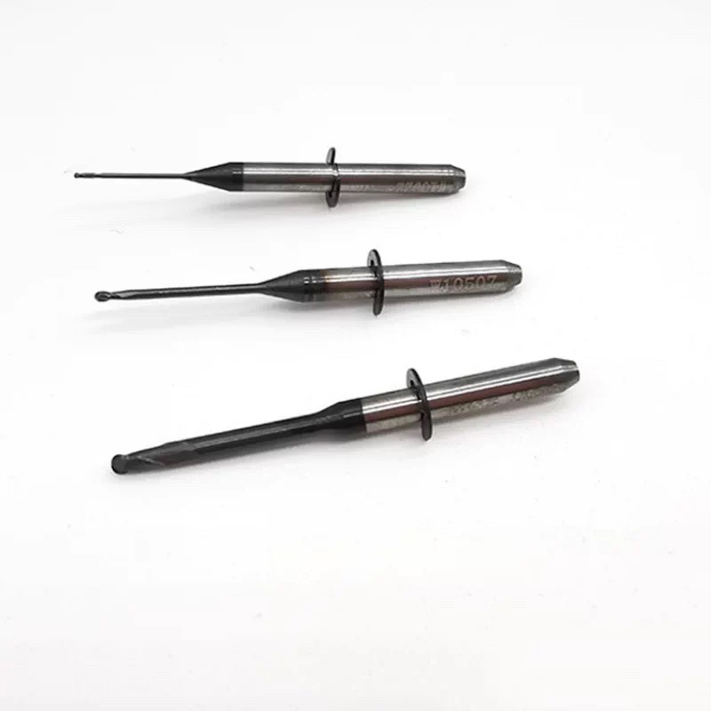
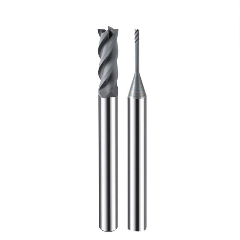
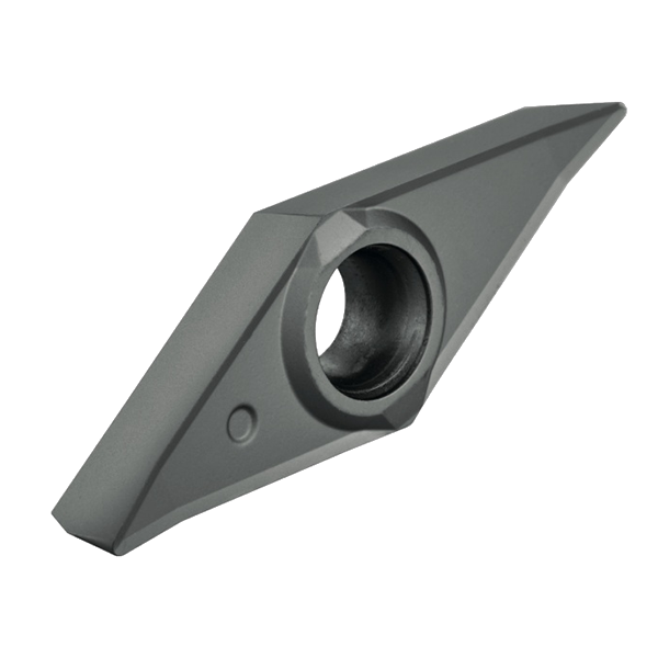
グラファイト、セラミック、カーボンファイバーは未来の素材だが、同時に「工具を駆逐する」存在でもある。もしあなたがまだ従来型のコーティングを使っているなら、負け戦を強いられていることになるだろう。
当社のCVD(化学気相成長法)ダイヤモンドコーティングは、炭化物基板上に本物の結晶ダイヤモンド層を形成します。これは単なる「表面処理」ではなく、保護膜としての役割を果たします。
トップディストリビューターが当社のCVDシリーズを選ぶ理由:
1.超低摩擦:切削屑の溶着や熱の蓄積を防ぎます。
2. 極めて高い耐摩耗性:切れ味の鋭さを20倍長く維持します。
3.表面仕上げ:加工対象物は鏡面仕上げとなり、二次研磨は不要です。